
RF DAC/ADC Module
Design & customization
Define a converter module around your signal chain. Discuss RF generation, high-speed acquisition, clocking and digital interfacing with MTT Innovations—from the first specification to an agreed customization scope.
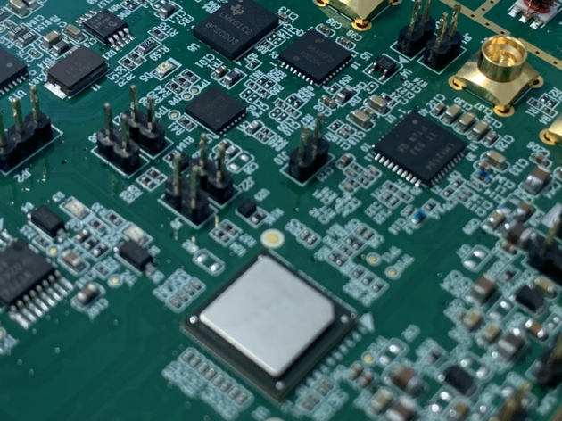
Connect the RF world.
Shape the digital signal.
Converter selection is only one part of the design. Channel count, clock distribution, RF bandwidth and the FPGA interface must work together. MTT can help structure your requirement and explore suitable module-level design options.
A starting point.
Your application comes next.
Explore the published reference hardware below, then discuss the changes your system needs.
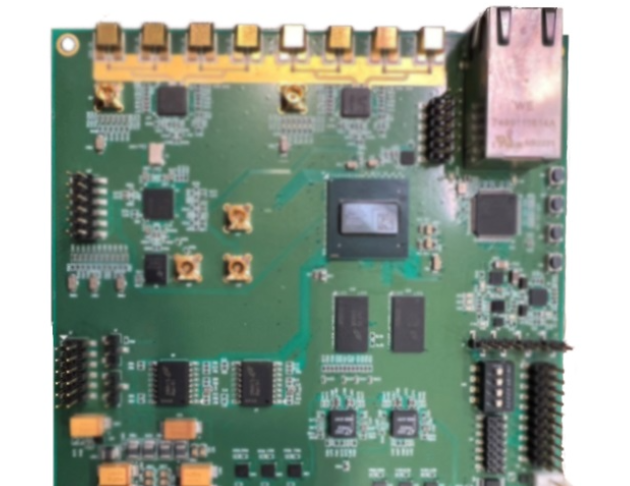
Four-channel RF generator · 12 GHz
A multi-output reference for synchronized RF generation, with an FPGA-based architecture and network control.
- Four RF outputs
- Frequency coverage up to 12 GHz
- Frequency and phase alignment
- UltraScale+ FPGA; Ethernet
Four-channel RF generator · 20 GHz
A higher-frequency generator reference for projects requiring multiple coordinated RF outputs.
- Four RF outputs
- Frequency coverage up to 20 GHz
- Frequency and phase alignment
- UltraScale+ FPGA; Ethernet
X-band ADC module
An acquisition-module reference combining a high-speed ADC, an integrated clock architecture and a serial digital interface.
- High-speed analog-to-digital conversion
- Clock architecture included
- JESD204B connectivity
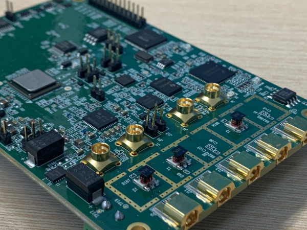
X-band receiver
A receiver reference incorporating digital down-conversion and clocking for connection to the digital processing chain.
- Digital down-conversion
- Clock architecture included
- JESD204B connectivity
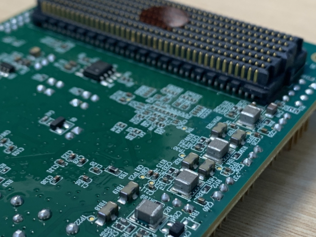
S-band DAC module
A high-speed conversion reference for the RF transmit path, with clocking and a converter-to-logic interface.
- High-speed digital-to-analog conversion
- Clock architecture included
- JESD204B connectivity
Specifications shown describe the individual reference designs, not every custom configuration. Final performance, interfaces and deliverables are agreed after technical review.
Define what your system needs.
RF architecture
Define transmit or receive operation, channel count, frequency coverage and the required analog signal path.
Clocking & coherence
Discuss reference-clock inputs, frequency and phase alignment, and timing relationships between channels.
Digital connectivity
Review JESD204B requirements, FPGA compatibility and the data path into the host system.
Mechanical integration
Specify connector positions, board outline, shielding, supply rails and thermal constraints.
Tell us what
success looks like.
Share the details you have, along with your target schedule and expected volume. We can use them to structure a technical discussion and identify the points that need further review.
Opens your email app with a ready-to-complete brief.
- 01Operating band and instantaneous bandwidth
- 02Number of DAC/ADC channels and sampling targets
- 03Resolution, dynamic-range and spectral-purity targets
- 04Clock reference, FPGA platform and digital interface
- 05Board dimensions, cooling and expected volume
From requirement to an agreed scope.
Share the application
Outline your signal chain, performance goals and integration constraints.
Assess the options
Review reference architectures and the feasibility of requested changes.
Set the project scope
Confirm specifications, engineering deliverables, commercial terms and schedule.
Plan the evaluation
Agree any prototype, test and acceptance activities required for the project.
Can the frequency range or channel count be changed?
Share the target range, bandwidth and channel count. Feasibility depends on the converter, RF signal path, clock architecture and selected processing platform.
Are converter resolution and dynamic range fixed?
No project values are assumed here. Specify the required resolution, ENOB, SFDR or other performance targets so they can be reviewed for the proposed configuration.
What information is needed for a quotation?
Send the technical brief, expected quantity, required deliverables and target schedule. Pricing and lead time depend on the agreed design, customization and evaluation scope.
Your requirement.
Our next conversation.
Connect with MTT Innovations to discuss rf dac/adc module design, customization and integration.