Electrical Specification and technical specifications
| Electrical Specification |
| Frequency Range |
1.5 to 30 MHz |
| BW (Typical) |
3.1% |
| Impedance (Input /Output) - Typical |
50 Ω |
| Fc±10% Selectivity - Typical |
< -28.5dBc |
| 2Fc |
< -60dBc |
| Tuning Speed |
< 20 µs |
| Insertion Loss Typical |
5.8 dB |
| Insertion Loss Max |
7.5 dB |
| Return Loss Min |
8.0 dB |
| Tuning Channels |
| 1.5MHz- 4MHz |
250 |
| 4.0MHz– 10MHz |
249 |
| 10MHz– 30MHz |
249 |
| RF Input Power (P1dB) |
| 1.5MHz to 4MHz |
33dBm |
| 4.0MHz to 10MHz |
33dBm |
| 10MHz to 30MHz |
33dBm |
| In Band Power Handing Max |
37dBm |
| Out of Band Power Handing |
37dBm |
| IP3 |
| 1.5MHz to 4MHz |
35dBm |
| 4MHz to 10MHz |
35dBm |
| 10MHz to 30MHz |
37dBm |
| Vcc |
3.3V~12V |
| Vbb |
NC |
| DC Current Max |
≤30mA |
| Operating Temperature Range |
-40 to +85°C |
| Control Interface |
SPI Interface |
| Dimensions |
2.2x2.2x0.5 inches (55.9x55.9x12.7 mm) |
Pin Designators and corresponding pin descriptions
| PIN DESIGNATORS |
| 1 |
GND |
14 |
GND |
| 2 |
RF IN |
15 |
SPI CLK |
| 3 |
GND |
16 |
SPI MOSI |
| 4 |
GND |
17 |
SPI CS |
| 5 |
N/C |
18 |
N/C |
| 6 |
N/C |
19 |
Vbb |
| 7 |
TUNE-READY |
20 |
GND |
| 8 |
N/C |
21 |
RV OUT |
| 9 |
N/C |
22 |
GND |
| 10 |
N/C |
23 |
GND |
| 11 |
N/C |
24 |
Vcc |
| 12 |
N/C |
25 |
GND |
| 13 |
GND |
|
|
N/C = NO CONNECT
NOTES:
1. TOLERANCES ±0.01 [0.25] UNLESS OTHERWISE SPECIFIED.
2. DIMENSIONS ARE INCHES [MM].
Available Bandwidths
Options available upon request Bandwidth options are available in increments of 1% step size.
Available bandwidth specifications for the 1.5 to 30 MHz frequency range
| Frequency Range |
| Available BW |
3.1% |
5% |
7% |
| *Ftune +/- 10% Selectivity (Typical) |
-28.5dBc |
TBD |
TBD |
| *Ftune +/- 15% Selectivity (Typical) |
-35.5dBc |
TBD |
TBD |
| *Ftune +/- 20% Selectivity (Typical) |
-41.0dBc |
TBD |
TBD |
| Insertion Loss (Typical) |
5.8 dB |
TBD |
TBD |
Corresponding Evaluation Board:
Model MTB20855 series filters are tunable band pass filters that can be tuned over the frequency
range of 1.5 to 30MHz. The MTB20855 Evaluation Board is designed to test and evaluate Model
MTB20855 frequency agile filter. The evaluation board will also work for future frequency agile
filters within the MTB20855 family. The evaluation board is used to supply power to the filter,
provide tuning control, facilitate measurement of the filter's RF parameters, switching speed, and
power consumption.
Tuning control of the filter is provided by the MTB20855 Evaluation Board in the form of frequency
tune words. The MTB20855 uses a USB input and user interface program to provide frequency
tuning control for the MTB20855 frequency agile filter. The MTB20855 Evaluation Board includes a
separate RF thru path for calibration of test equipment to improve the accuracy of RF
measurements.
Serial Address Input Timing Diagram:
When the SPI_CS line is shifted low, the Tune Ready line will be at a high logic state indicating the
unit is ready to accept the tune word. Tuning of the filter starts when the last data clock (16th) pulse
of the address is sent to the unit while the SPI_CS (Chip Select) is low. When the filter tuning is
complete, the Tune Ready line will go to a high logic state. Reset the SPI_CS line high after sending
the 16th clock pulse to allow the unit to reset after the filter tuning is complete.
Serial Address Input Timing Parameters
| Symbol |
Parameter |
Min |
Max |
Units |
| tSS |
Setup time MOSI Data to SPICLK |
50 |
|
ns |
| tu |
Hold Time MOSI Data From SPICLK |
|
0 |
ns |
| tCH |
Clock High Time |
125 |
|
ns |
| tCP |
Clock Period |
250 |
|
ns |
| tCS |
Chip Setup Time (CS falling edge to SPICLK start) |
125 |
|
ns |
| tTR |
Tune Ready Indicator |
|
200 |
us |
| tACC |
Access time from Last (16th) SPICLK edge to Fo |
|
200 |
us |
| |
Maximum Hop Rate Tune Frequency to next Tuned Frequency |
|
1000 |
Hz |
Bit Map showing Band Switch Byte and Address Byte
| Bit Map |
| Band Switch Byte |
Address Byte |
D15
MSB |
D14 |
D13 |
D12 |
D11 |
D10 |
D9 |
D8 |
D7 |
D6 |
D5 |
D4 |
D3 |
D2 |
D1 |
D0 |
| 0 |
0 |
0 |
0 |
0 |
0 |
0 |
B1* |
B0* |
Filter Tune Address** |
*Refer to Band Switch Table for B1 and B0 codes of Band Switch Byte.
** Refer to Address Table for selected band start and end addresses.
Band Switch Table:
Band Switch Table
| Band |
B1 |
B0 |
Frequency Range |
| 1 |
0 |
0 |
1.5MHz - 4.0MHz |
| 2 |
0 |
1 |
4.0MHz - 10.0MHz |
| 3 |
1 |
0 |
10.0MHz - 30.0MHz |
| Illegal Selection |
1 |
1 |
Do Not Select |
Address Table:
Address Table
| Band |
Start Address |
End Address |
Frequency Range |
| 1 |
0 |
250 |
1.5MHz - 4.0MHz |
| 2 |
0 |
249 |
4.0MHz - 10.0MHz |
| 3 |
0 |
249 |
10.0MHz - 30.0MHz |
Environmental Specification Standards
| Environmental Specification Standards: |
| Temperature |
- High temperature shall meet MIL-STD-810E, Method 501.3, Procedure I to 85°C storage, and procedure II to 85°C operating.
- Low temperature shall meet Method 502.3, Procedure I to -57°C storage, and Procedure II to -40°C operating.
|
| Vibration |
MIL-STD-810E Method 514.4 Ground Mobile Test Procedure I, Test Condition I - 3.4.7
|
| Shock |
MIL-STD-810E Procedure I, Method 516.4 - Functional Shock.
|
| Reflow |
218°CMax (30 seconds) MSL (Moisture Sensitivity Level: Level 3
|

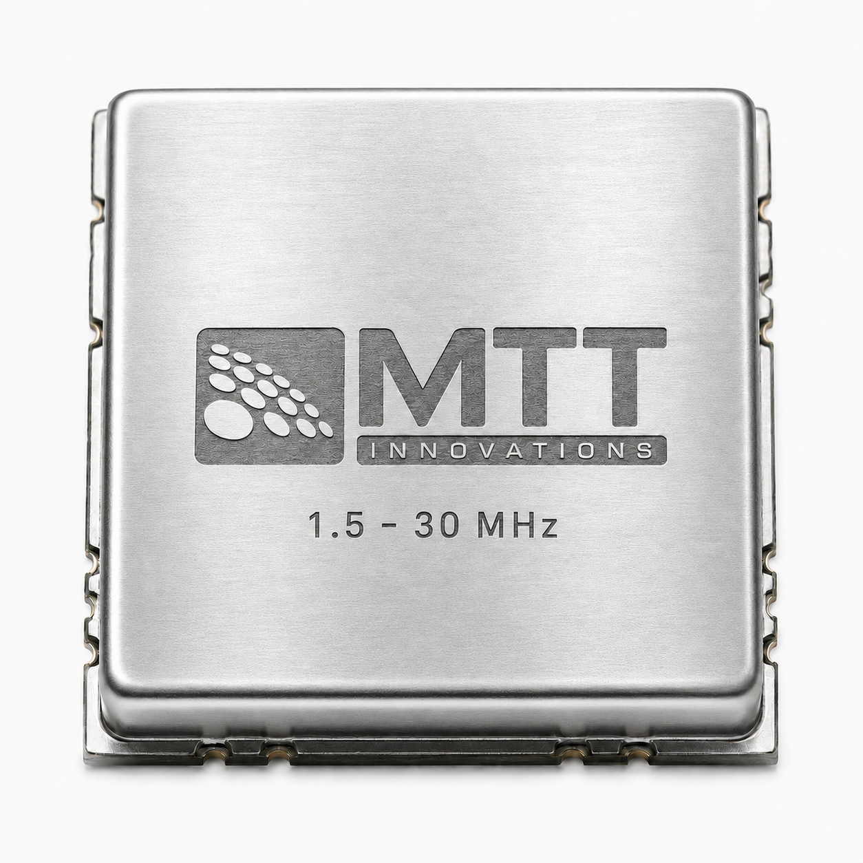 Image 1 of 2
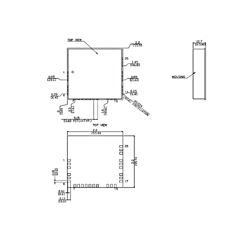 Image 2 of 2