 Image 1 of 1
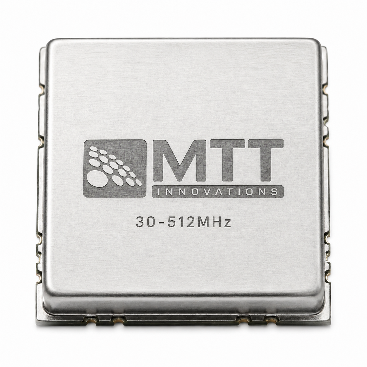
30–512 MHz Chip Tunable Filter
Frequency-agile RF filtering across three selectable bands with ≥2% relative bandwidth, ≥13 dBc rejection at F0 ±5%, ≥27 dBc at F0 ±10%, 10-bit parallel control and tuning in 5 µs or less.

One compact filter covering VHF through UHF.
The MTT3051X-7-J combines three digitally selectable frequency bands, ≥2% relative bandwidth, ≥13 dBc rejection at F0 ±5% and ≥27 dBc rejection at F0 ±10%, 8-bit in-band tuning and a shielded 17-pin package for integration into frequency-agile radios, receivers and RF test platforms.
Three selectable bands
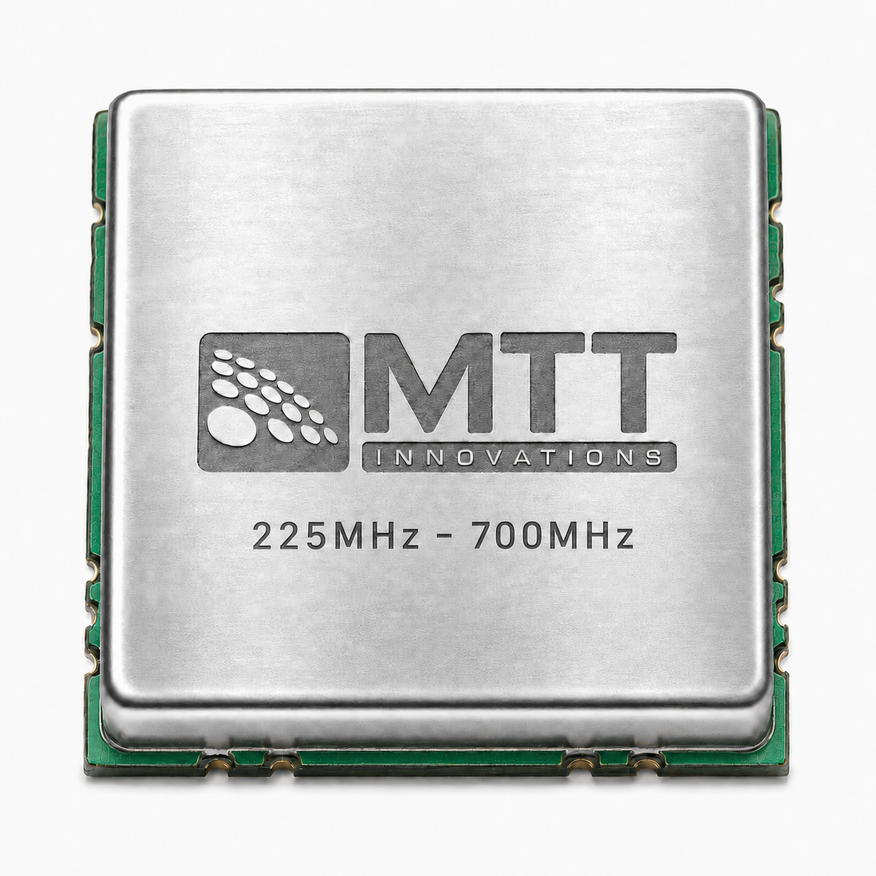
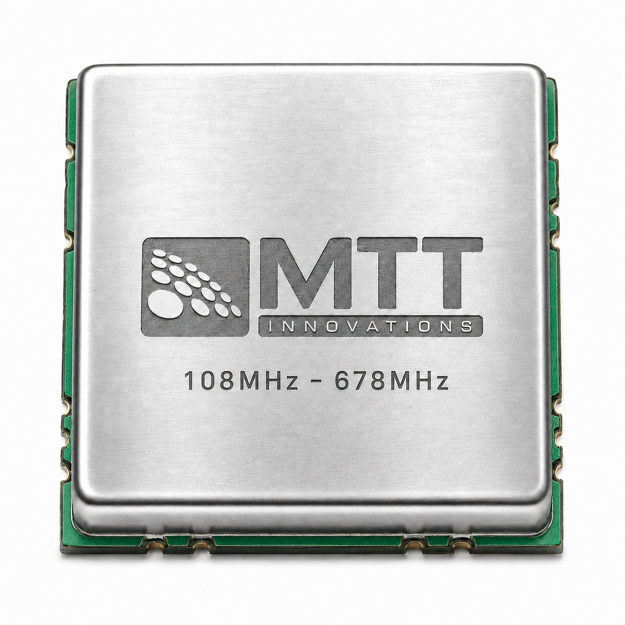
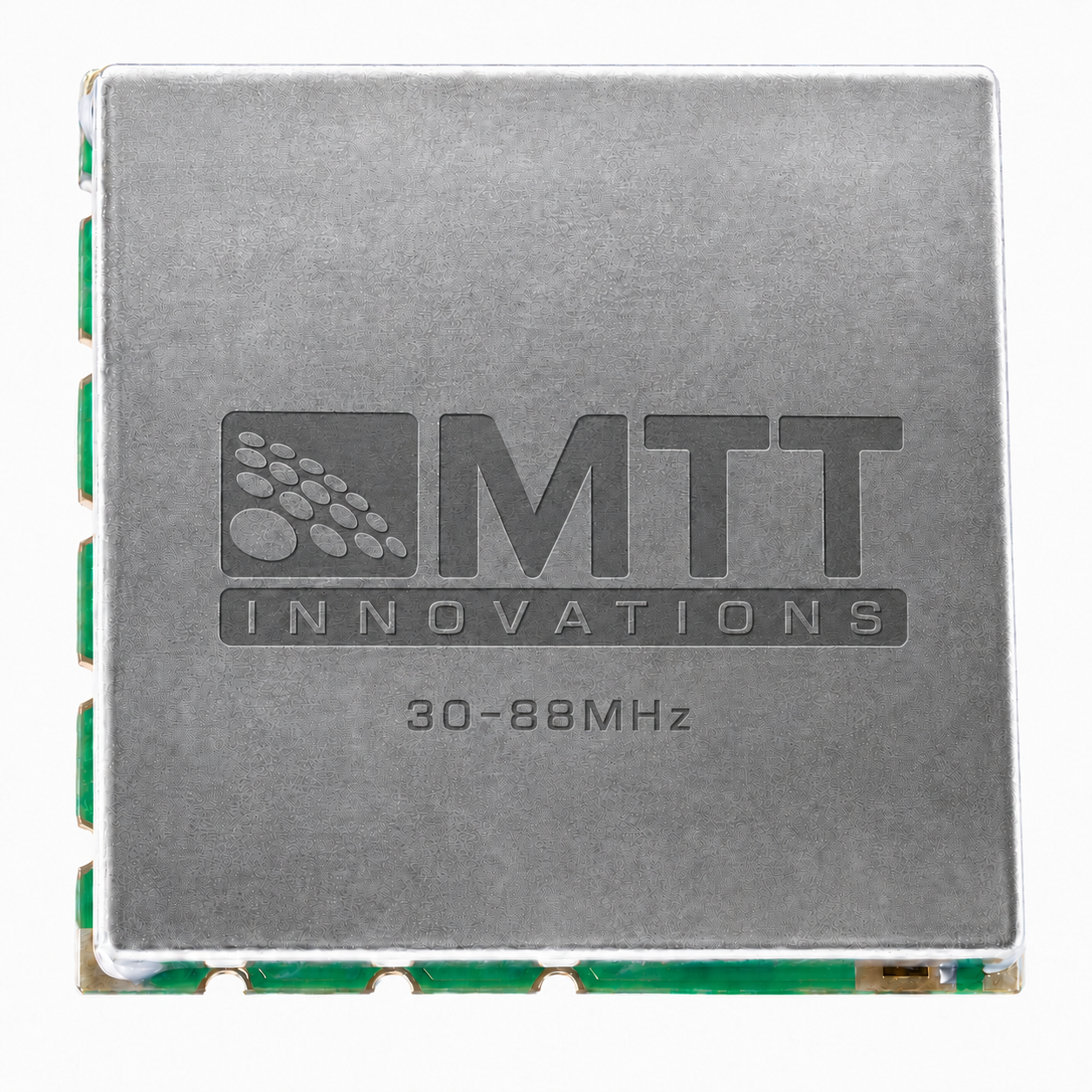
Band-control inputs select 30–90 MHz, 90–225 MHz or 225–512 MHz operation.
10-bit parallel interface
A0–A7 set the in-band address while A8–A9 select the operating band, with CMOS and TTL-compatible logic levels.
Wide temperature operation
Specified from −40 °C to +85 °C, with storage capability from −55 °C to +105 °C.
Electrical specifications
Values below are reproduced from datasheet revision A-0 and apply over the stated −40 °C to +85 °C specification range.
| Parameter | Symbol | Specification |
|---|---|---|
| Frequency range | F | 30–90 MHz; 90–225 MHz; 225–512 MHz |
| Insertion loss | I.L | ≤ 7 dB |
| −1 dB bandwidth | BW−1 | ≥ 2% × F0 |
| Out-of-band rejection | Sel. | F0 ±5%: ≥ 13 dBc; F0 ±10%: ≥ 27 dBc |
| RF input power | P(−1 dB) | ≤ 35 dBm |
| Tuning time | Tv | ≤ 5 µs |
| VSWR | VSWR | ≤ 1.5 |
| Input / output impedance | Zin / Zout | 50 Ω |
| Supply voltage | Vs | +3.3 V to +12 V |
| Power consumption | P | ≤ 50 mW |
| Center-frequency drift | F0 drift | ≤ 80 ppm/°C |
| Operating temperature | To | −40 °C to +85 °C |
| Storage temperature | Ts | −55 °C to +105 °C |
| Weight | W | ≤ 20 g |
| Dimensions | — | 38.1 × 25.4 × 6 mm (±0.2 mm) |
F0 denotes the selected center frequency. Confirm final test conditions and revision status with MTT before design release.
Band selection and address control
The 10-bit parallel interface uses A0–A7 for in-band tuning and A8–A9 for frequency-band selection.
Address-code definition
10-bit parallel binary code A0–A9, compatible with CMOS and TTL logic levels.
Address calculation
Calculate the in-band address within the selected segment, then round any decimal result to the nearest integer.
- fx
- Desired intra-segment center frequency
- flow
- Lowest frequency in the selected segment
- fhigh
- Highest frequency in the selected segment
- 250
- Number of intra-segment steps stated in the datasheet
Pin assignment and package
Bottom-view pin naming is reproduced from the mechanical drawing. Verify orientation against the controlled drawing before PCB release.
17-pin definition
RF, band selection, tuning control, power and ground connections
Mechanical summary
Nominal data from datasheet revision A-0
Use the controlled mechanical drawing for PCB land-pattern design, pin orientation and manufacturing tolerances.
Select your 30–512 MHz filter variation
Compare bandwidth, RF input rating and package format. The product you are viewing is highlighted below.
Compact 17-pin modules
27-pin modules with higher-power option
Need samples, pricing, or engineering support?
Share your requirement with MTT. After submitting your details, you can immediately download the product datasheet.
Tell us about your requirement.
Complete the short enquiry form. Your datasheet download will be available immediately after successful submission.
Thank you for your enquiry.
Your details have been received. Use the button below to download the MTT3051X-7-J datasheet.
Download Datasheet →MTT3051X-7-J · 30–512 MHz Chip Tunable Filter · Datasheet Revision A-0 · Specifications are subject to confirmation at the time of order.