
 Image 1 of 1
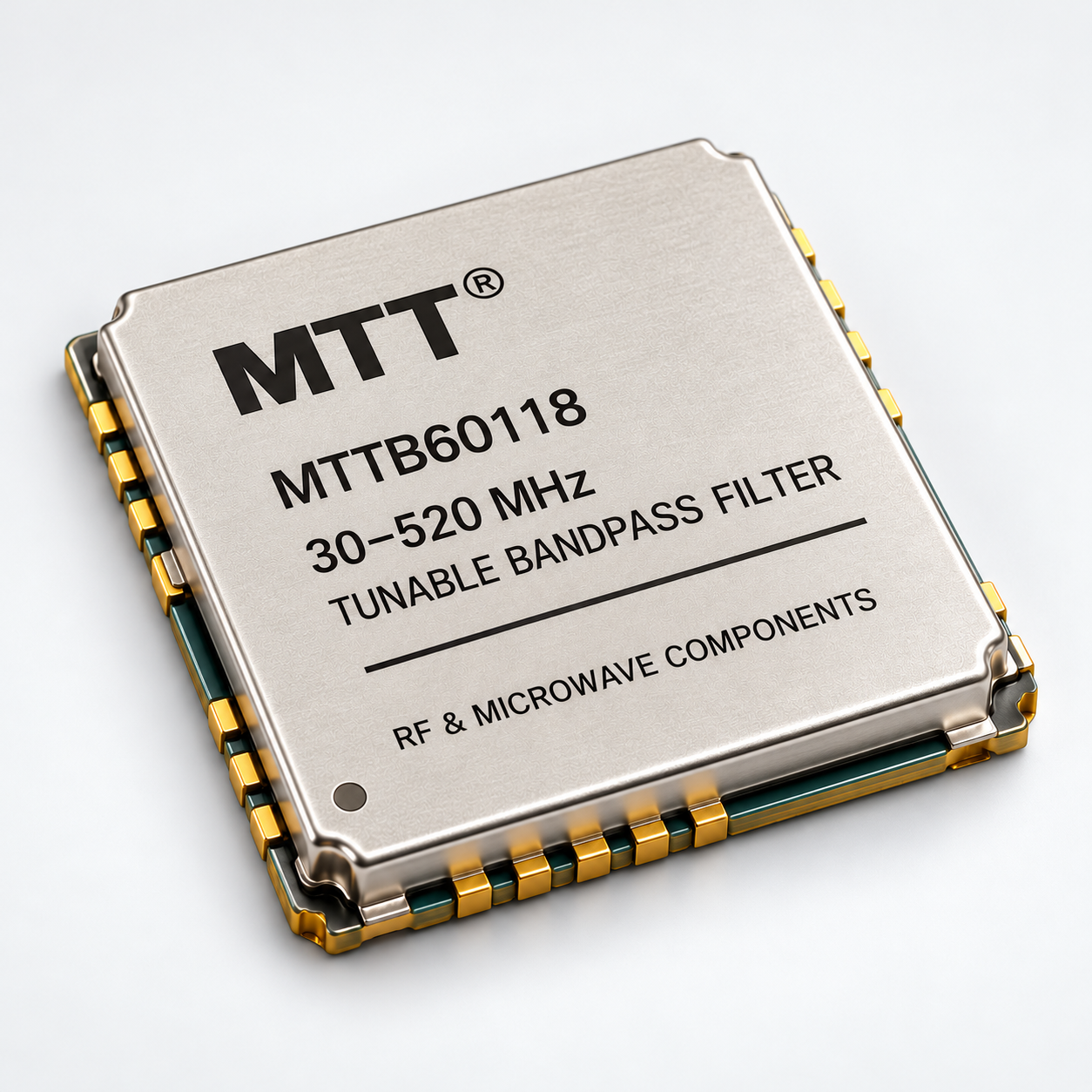
30–520 MHz Tunable Bandpass Filter
10 mm SMT Package
Compact, frequency-agile VHF/UHF RF filtering with SPI digital control, 5 dB typical insertion loss and +45 dBm typical IIP3.
Product overview
Engineered for agile VHF/UHF RF chains
MTTB60118 is a digitally tunable 30–520 MHz bandpass filter in a 10 mm-high surface-mount package. The source identifies uses in tactical radios, transmit paths and receiver chains.
Size: 22.1 × 22.1 × 10 mm · Supply: 3.3 V nominal · SPI: 16-bit tuning interface.
Important RF power interpretation
+33 dBm typical P1dB is a 1 dB compression point, not automatically a continuous 2 W input-power rating. Power handling and switching conditions should be confirmed for the intended application.
Out-of-band limit: +37 dBm maximum stated in source.
Complete electrical and RF specifications
| Parameter | Min | Typical | Max / note |
|---|---|---|---|
| Tunable frequency | 30 MHz | — | 520 MHz |
| 3 dB bandwidth | 4% | 5.0% | 6% |
| Rejection at f₀ ±10% | — | -26 dB | — |
| Rejection at f₀ ±15% | — | -32 dB | — |
| Rejection at f₀ ±20% | — | -36 dB | — |
| Insertion loss | — | 5.0 dB | — |
| RF impedance | — | 50 Ω | — |
| Typical tune speed | — | 20 µs | 30 µs max. |
| P1dB | +30 dBm | +33 dBm | +35 dBm |
| Out-of-band power | — | — | +37 dBm |
| IIP3 (+18 dBm two-tone, ±5 kHz) | — | +45 dBm | — |
| Noise figure | — | IL + 0.5 dB | IL + 5 dB |
| Wideband noise | — | -174 dBm/Hz | — |
| Supply voltage | 3.0 V | 3.3 V | 3.6 V |
| DC current | — | 15 mA | 20 mA |
| Operating temperature | −40°C | — | +75°C |
| Control | — | 16-bit SPI serial | — |
| C tuning option | — | 125 kHz nominal (variable step by band) | — |
| D tuning option | — | 1 MHz | — |
| Package dimensions | — | 22.1 × 22.1 × 10 mm | — |
Values transcribed from the 10 mm model source (p.2). Refer to original measurement definitions and option codes; unspecified values are intentionally not inferred.
Functional block and RF signal routing
The source functional diagram shows RF input/output, three selected tunable filter paths and associated control/power pads. Preserve the model-specific 23-pin configuration in PCB designs.
Tuning modes, addressing and bypass
C option: fine addressing
The source calls this the “125 kHz tuning step” option, with step sizes that change across the band.
| Address interval | Frequency interval | Step |
|---|---|---|
| 240–511 | 30–63.875 MHz | 125 kHz |
| 512–1022 | 64–127.750 MHz | 250 kHz |
| 1024–2044 | 128–255.500 MHz | 500 kHz |
| 2048–4160 | 256–520 MHz | 1 MHz |
D option: 1 MHz addressing
Decimal addresses 30 through 520 select frequencies from 30 MHz to 520 MHz in 1 MHz increments. The device begins tuning when the sixteenth SCLK data pulse is clocked while CS is low.
Bypass command: 0xFF00 as stated in the source; resume normal operation by sending a valid tuning address. Confirm the option before deploying this command.
The original source includes address discontinuities and defines unused channels only by implication. Do not generate unsupported addresses.
SPI timing and serial behaviour
Data is clocked on the leading SCLK edge. The source describes TUNE_READY as low while the module processes a new tuning address. For the specific min/max entries and waveforms, use the timing diagram below.
| Symbol | Definition | Source rating |
|---|---|---|
| tSS | MOSI setup to SCLK | 50 ns min. |
| tu | MOSI hold after SCLK | 0 ns max. as tabulated |
| tCH | Clock high time | 125 ns min. |
| tCP | Clock period | 250 ns min. |
| tCS | Chip-select setup to SCLK | 125 ns min. |
| tTR | Tune Ready indicator | 30 µs max. |
| tACC | Access time, final SCLK to RF frequency | 30 µs max. |
| tHOP | Frequency-to-frequency tune rate (D-option) | 11 kHz max. as source states |
Mechanical outline, PCB land pattern and pinout
Mechanical envelope: 22.1 mm × 22.1 mm × 10 mm. Preserve pin-1 orientation, castellation geometry and solder land dimensions from the model-specific drawing.
| Pin | Signal / label |
|---|---|
| 1 | GND |
| 2 | N/C |
| 3 | N/C |
| 4 | GND |
| 5 | RF_IN |
| 6 | GND |
| 7 | TUNE_READY |
| 8 | N/C |
| 9 | N/C |
| 10 | N/C |
| 11 | SD0 |
| 12 | GND |
| 13 | +3.3V |
| 14 | SCLK |
| 15 | MOSI |
| 16 | GND |
| 17 | RF_OUT |
| 18 | GND |
| 19 | CS |
| 20 | N/C |
| 21 | GND |
| 22 | GND |
| 23 | GND |
Pin 11 is labelled SD0 in this model’s source. The 5 mm and 10 mm PDFs show “SD0”, while the 7 mm PDF shows “SDO”. Confirm the intended designation before PCB release.
Environment, compliance and handling
| Item | Source specification / instruction |
|---|---|
| Operating temperature | −40 to +75°C in electrical table (p.2) |
| MIL-STD-810E high temperature | 75°C high-temperature operation in environmental table (source p.6). |
| MIL-STD-810E storage high | 125°C, Method 501.3, Procedure I |
| MIL-STD-810E storage low | −57°C, Method 502.3, Procedure I |
| Vibration | MIL-STD-810E, Method 514.4 |
| Shock | MIL-STD-810E, Method 516.4, Procedure VI |
| RoHS | Source states compliant |
| Plating | Electroless nickel 100 µin minimum; immersion gold 2–6 µin on outer layers |
| Moisture sensitivity | MSL 3 |
| Cleaning | ODC-compatible solvents; avoid methylene chloride/epoxy solvents; no ultrasonic cleaning; keep dry before assembly |
The source wording includes a legacy reference to “Netcom” in the cleaning guidance. This is not presented here as an MTT certification or independent test evidence.
Solder reflow and assembly guidance
The supplied PDF provides separate SnPb and Pb-free soldering windows. Actual reflow characteristics depend on PCB thickness, paste, thermal mass and neighbouring devices. Temperatures are specified at the PCB interface.
| Parameter | SnPb | Pb-free |
|---|---|---|
| Ramp-up | 3°C/s max. | 3°C/s max. |
| Preheat TSMIN | 100°C | 150°C |
| Preheat TSMAX | 150°C | 200°C |
| Preheat time | 60–120 s | 60–120 s |
| Solder melting point | 183°C | 217°C |
| Peak temperature | 225°C | 245°C |
| Time above liquidus | 45–90 s | 45–70 s |
| Within 5°C peak | 30 s max. | 30 s max. |
| Ramp-down | 6°C/s max. | 6°C/s max. |
| 25°C to peak | 4.5 min max. | 5 min max. |
Request the complete 10 mm datasheet
Send the MTT technical team an enquiry for MTTB60118 — 30–520 MHz Tunable Bandpass Filter (10 mm).