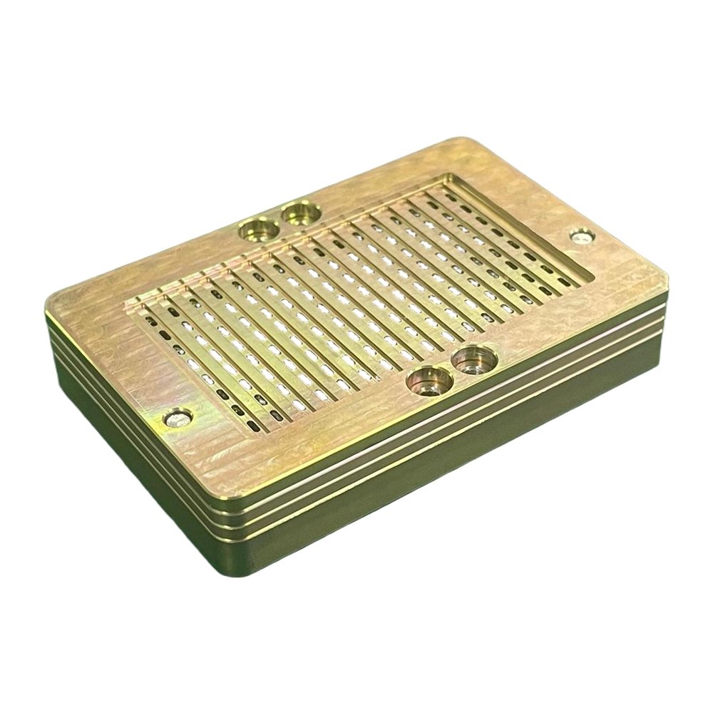
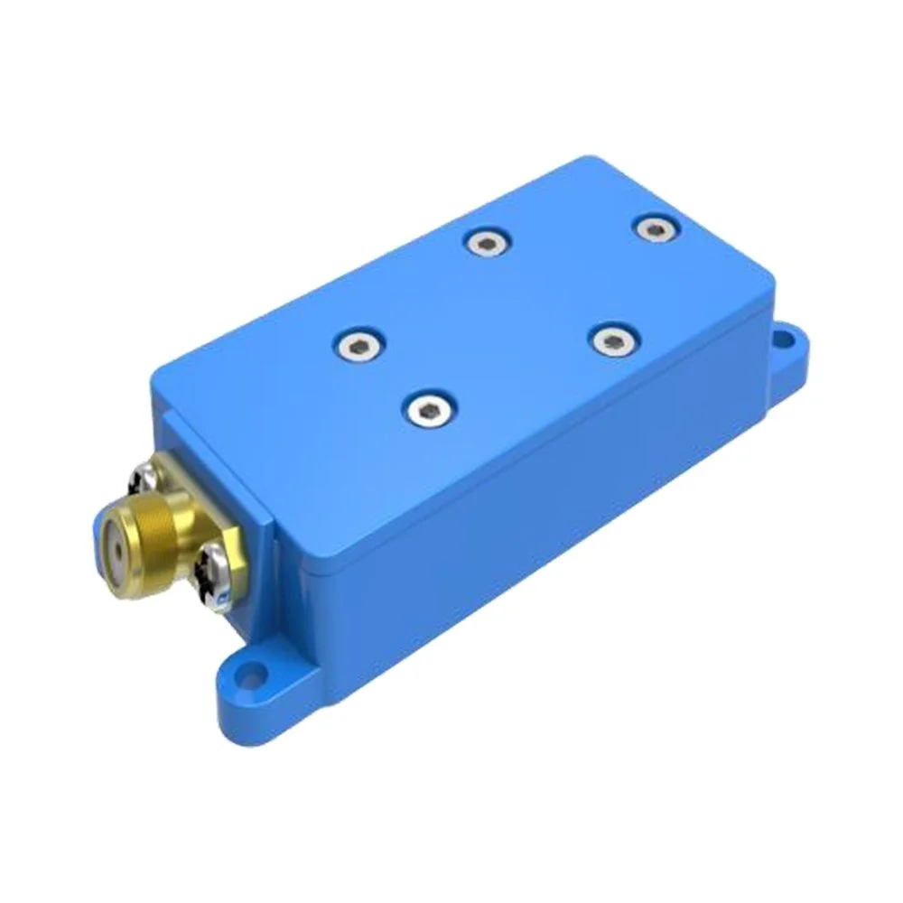
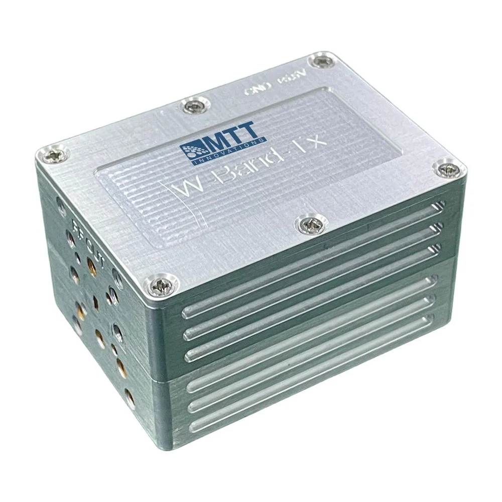
 Image 1 of 3
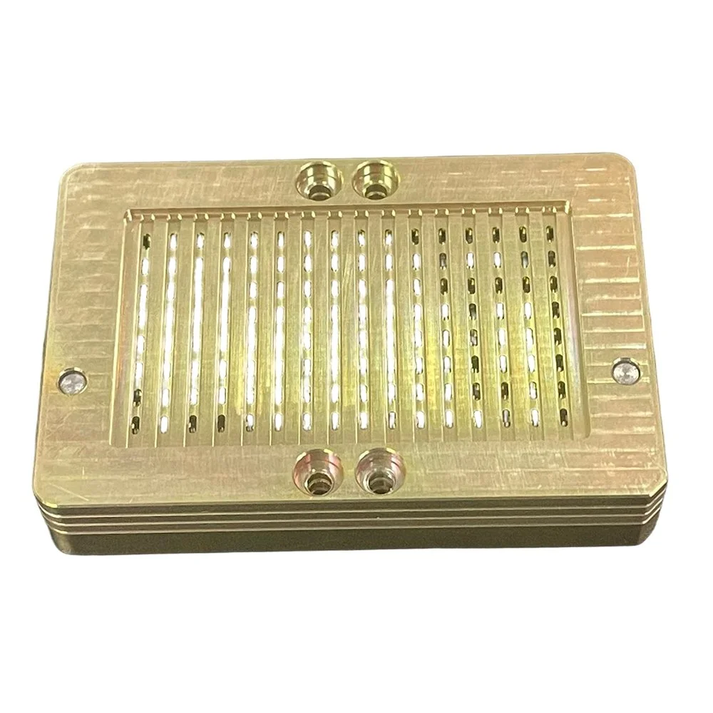
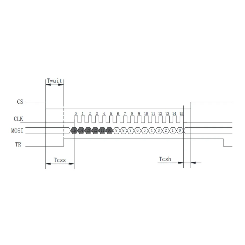
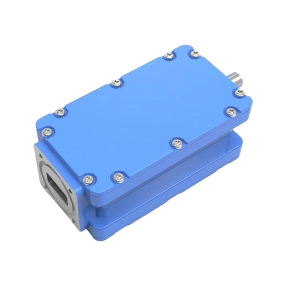
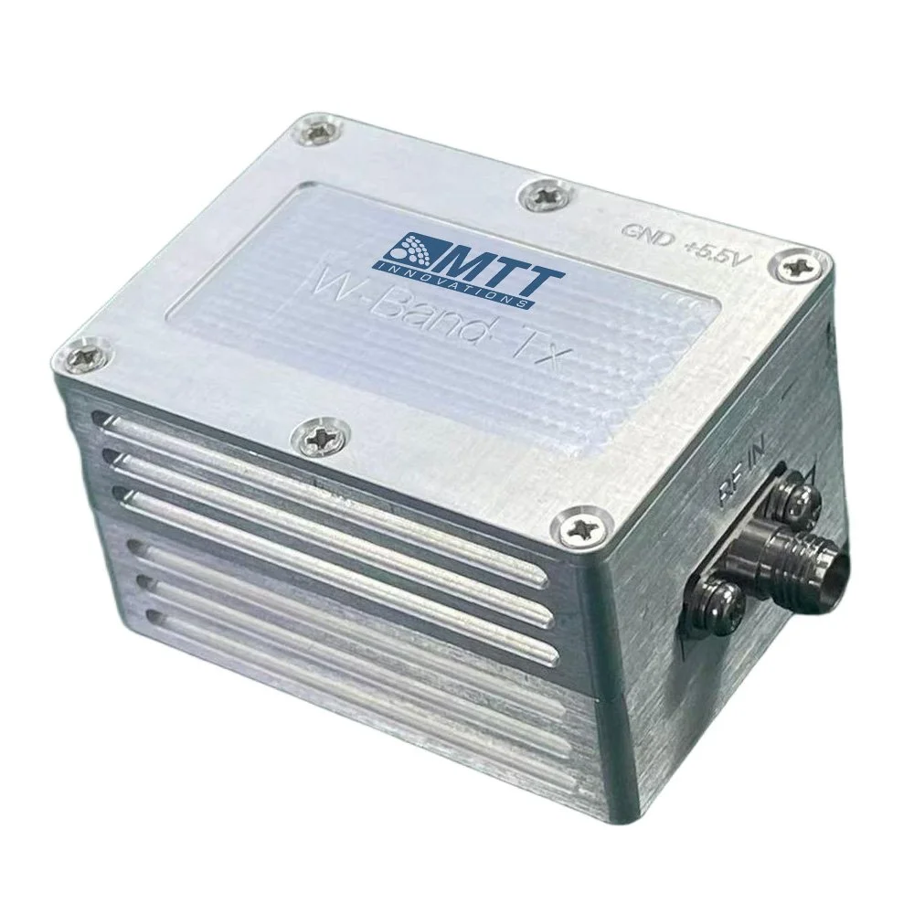 Image 2 of 3
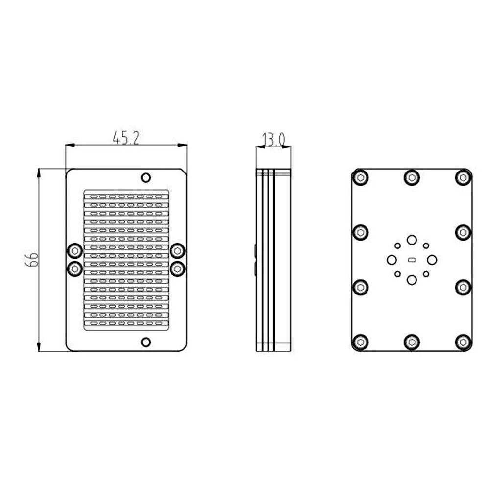
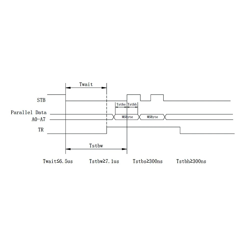
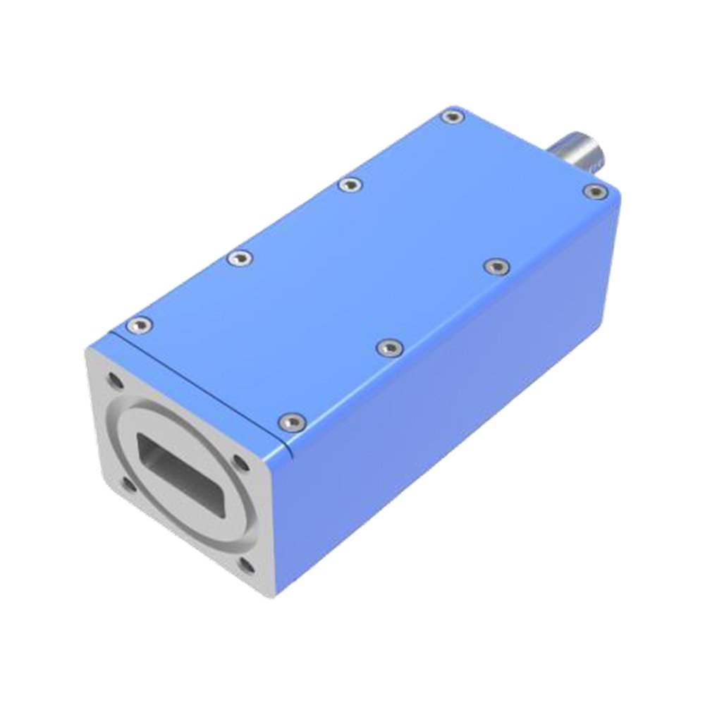
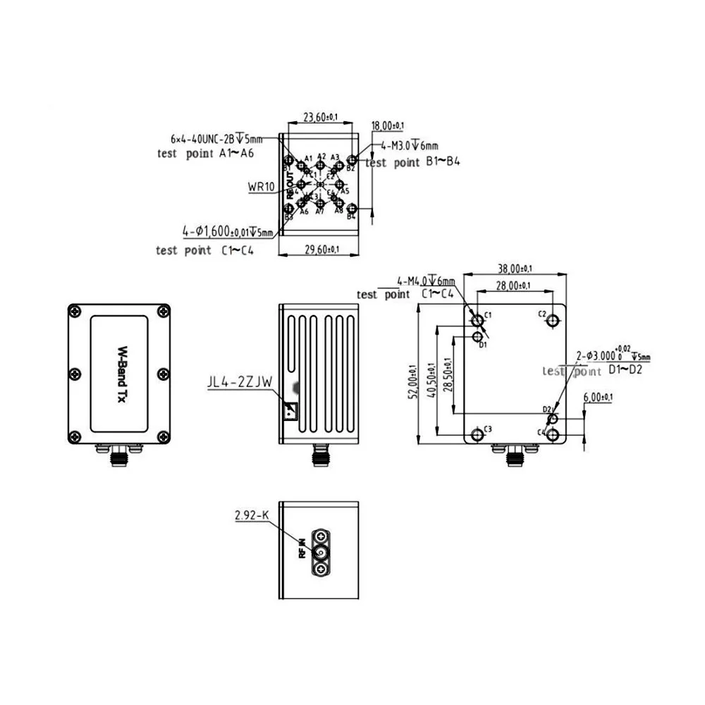 Image 3 of 3
Electrical Specifications
| Parameter | Min | Typ | Max | Unit |
|---|---|---|---|---|
| Frequency | 92 | - | 94 | GHz |
| Bandwidth | - | 2 | - | GHz |
| Input Frequency | 11.5 | - | 11.75 | GHz |
| Output Power | 20 | - | - | dBm |
| Output Power Flatness | - | ≤1.5 | - | dB |
| Spurs | - | ≤45 | - | dBc |
| Power Variation at High Humidity | - | ≤1.5 | - | dB |
| Input Power | 2 | - | 8 | dBm |
Performance Specifications
| Parameter | Maximum Rating |
|---|---|
| Input Power | +10 dBm (CW) |
| Operating Voltage | +6.5 V |
| Operating Temperature | -40 ℃ to +85 ℃ |
| Storage Temperature | -55 ℃ to +85 ℃ |
Recommended Operating Conditions
| Parameter | Min | Typ | Max | Unit |
|---|---|---|---|---|
| Input Power (CW) | +2 | 5 | +8 | dBm |
| Operating Voltage (Vd) | 5 | 5.5 | 6 | VDC |
| Operating Temperature | -32 | - | +75 | ℃ |
| Operating Current | 0.5 | - | - | A |
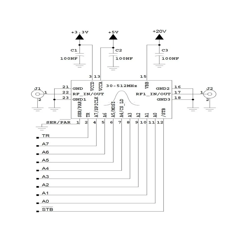
Interface Definition
| Interface | Pin No. | Name | Attribute |
|---|---|---|---|
| JL4-2ZJW | 1 | VDD | +5.5V |
| JL4-2ZJW | 2 | GND | - |
| 2.92-Female | - | FRIN | RF Input |
| WR10 | - | FROUT | RF Output |