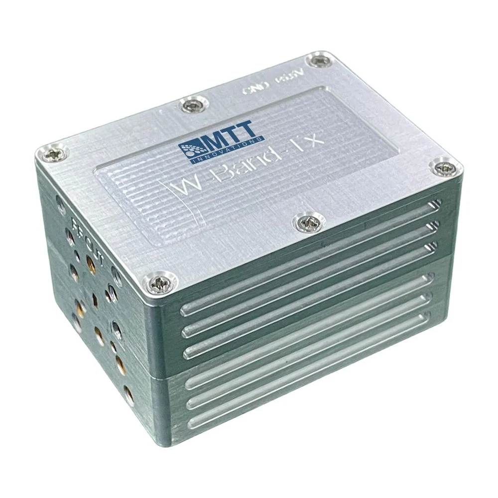
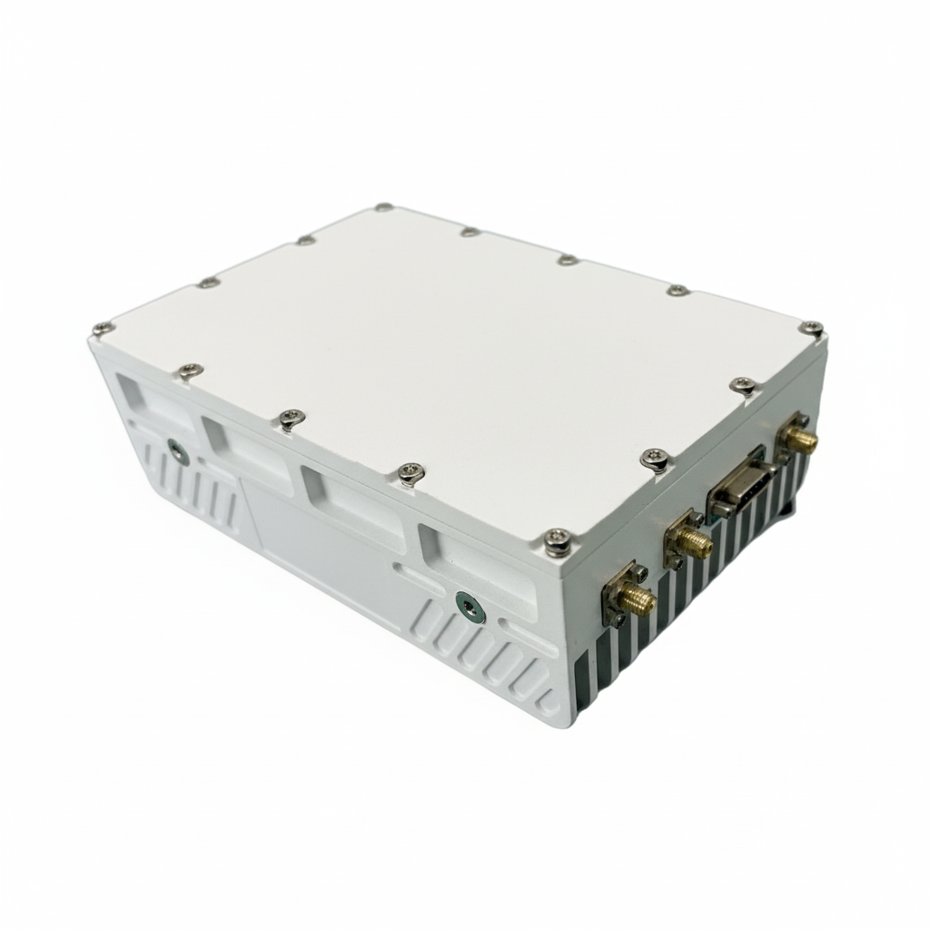
 Image 1 of 9
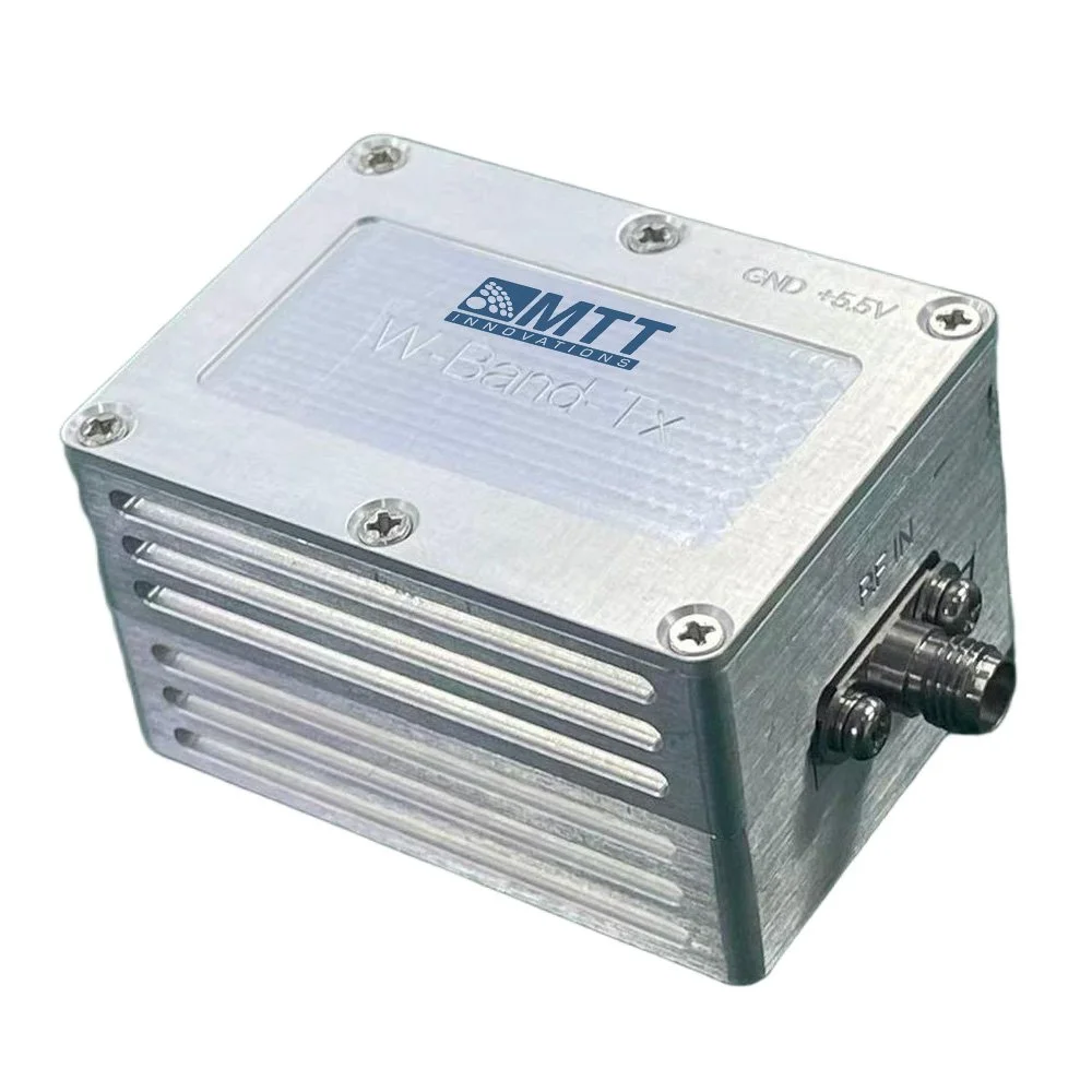
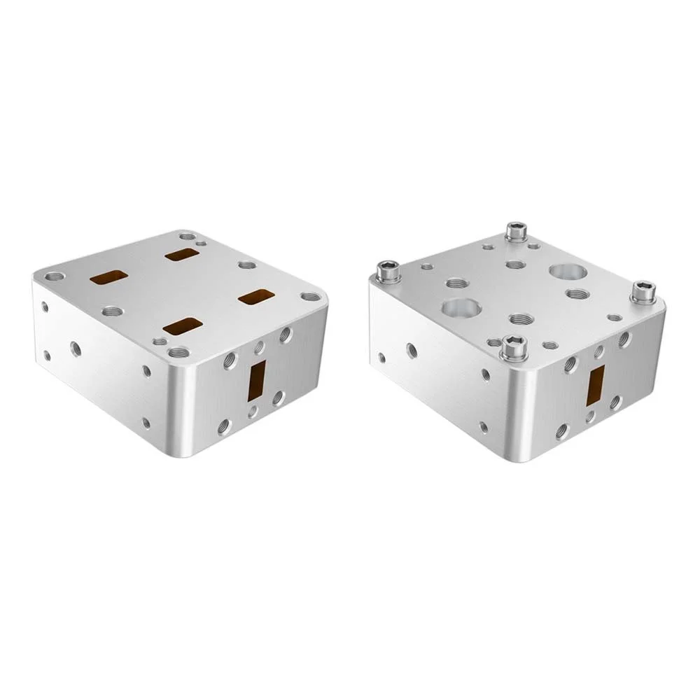
 Image 2 of 9
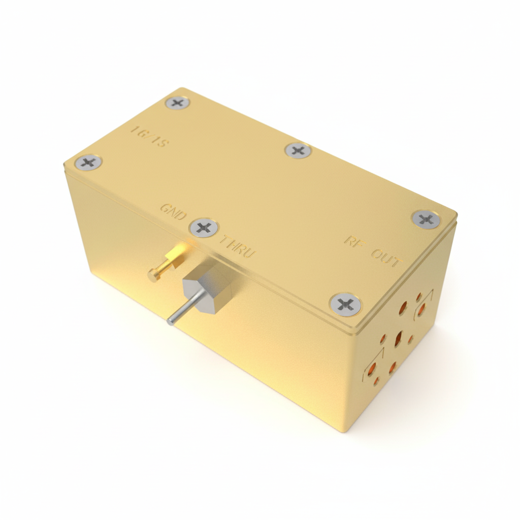
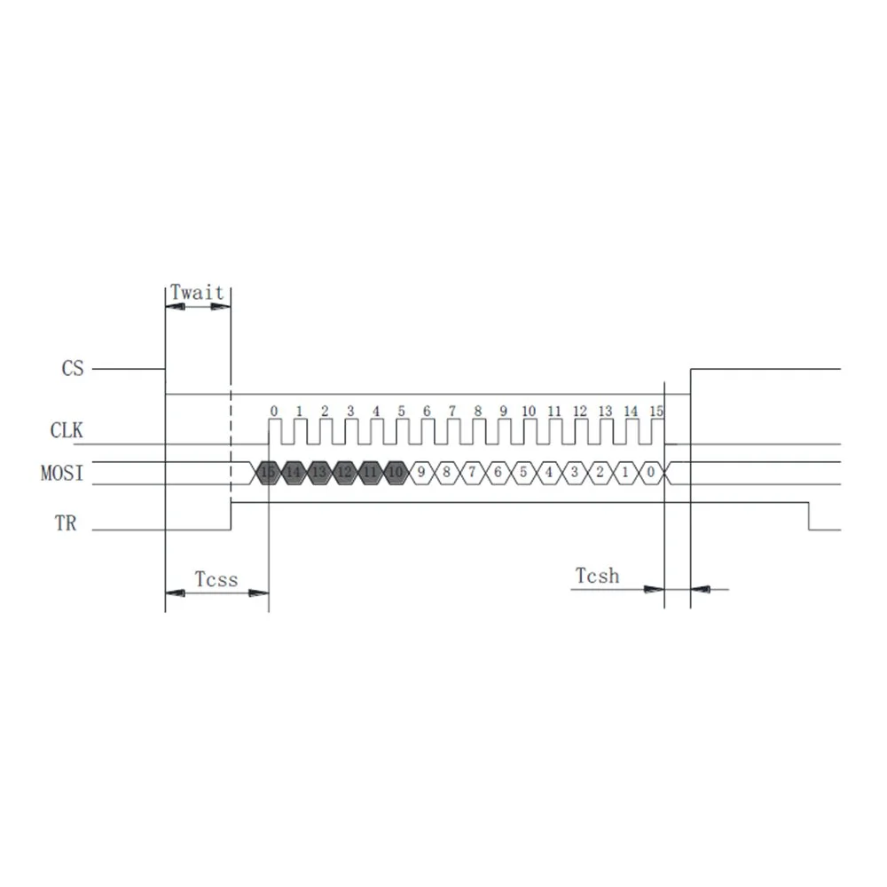 Image 3 of 9
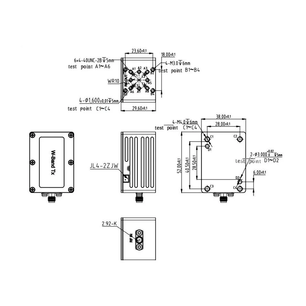
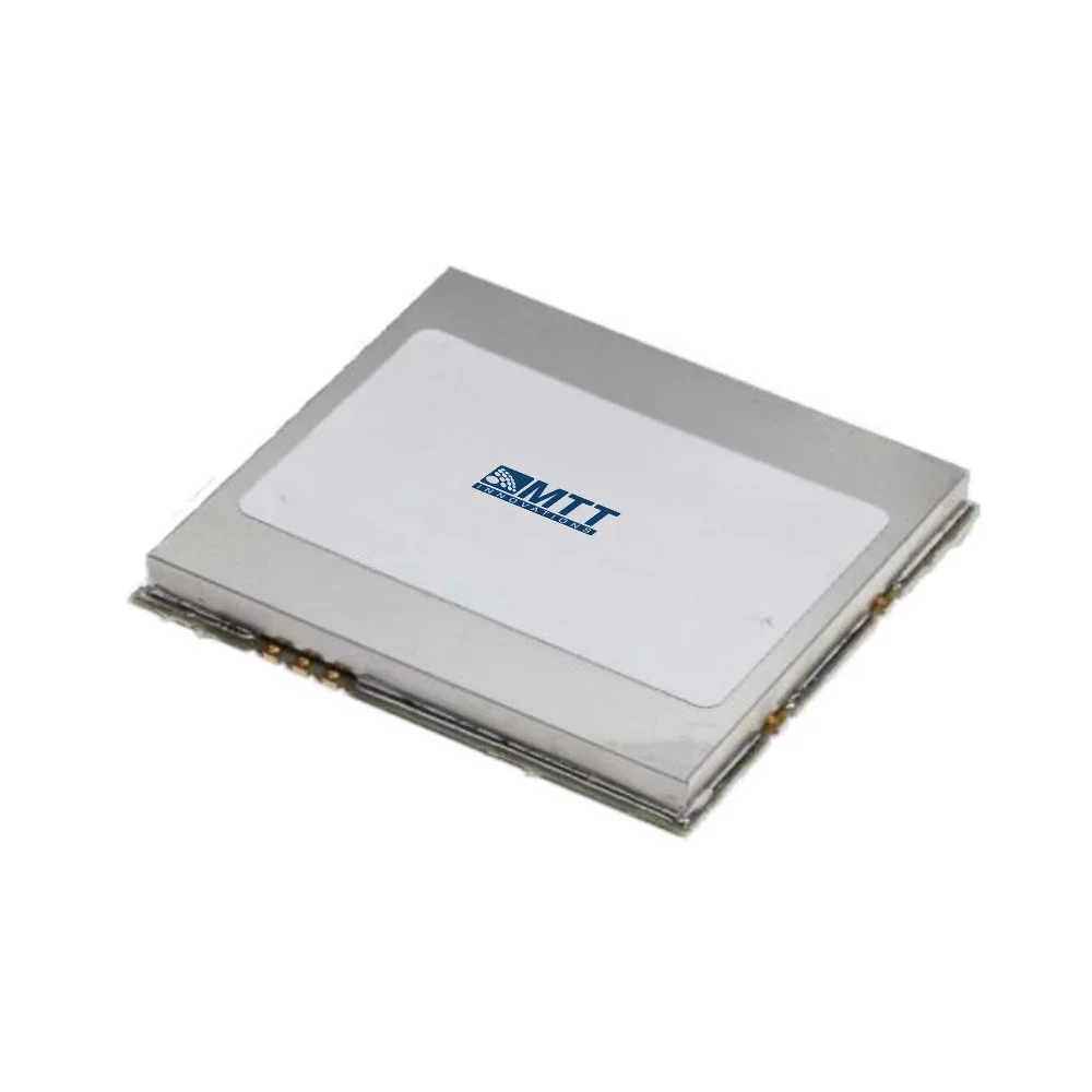
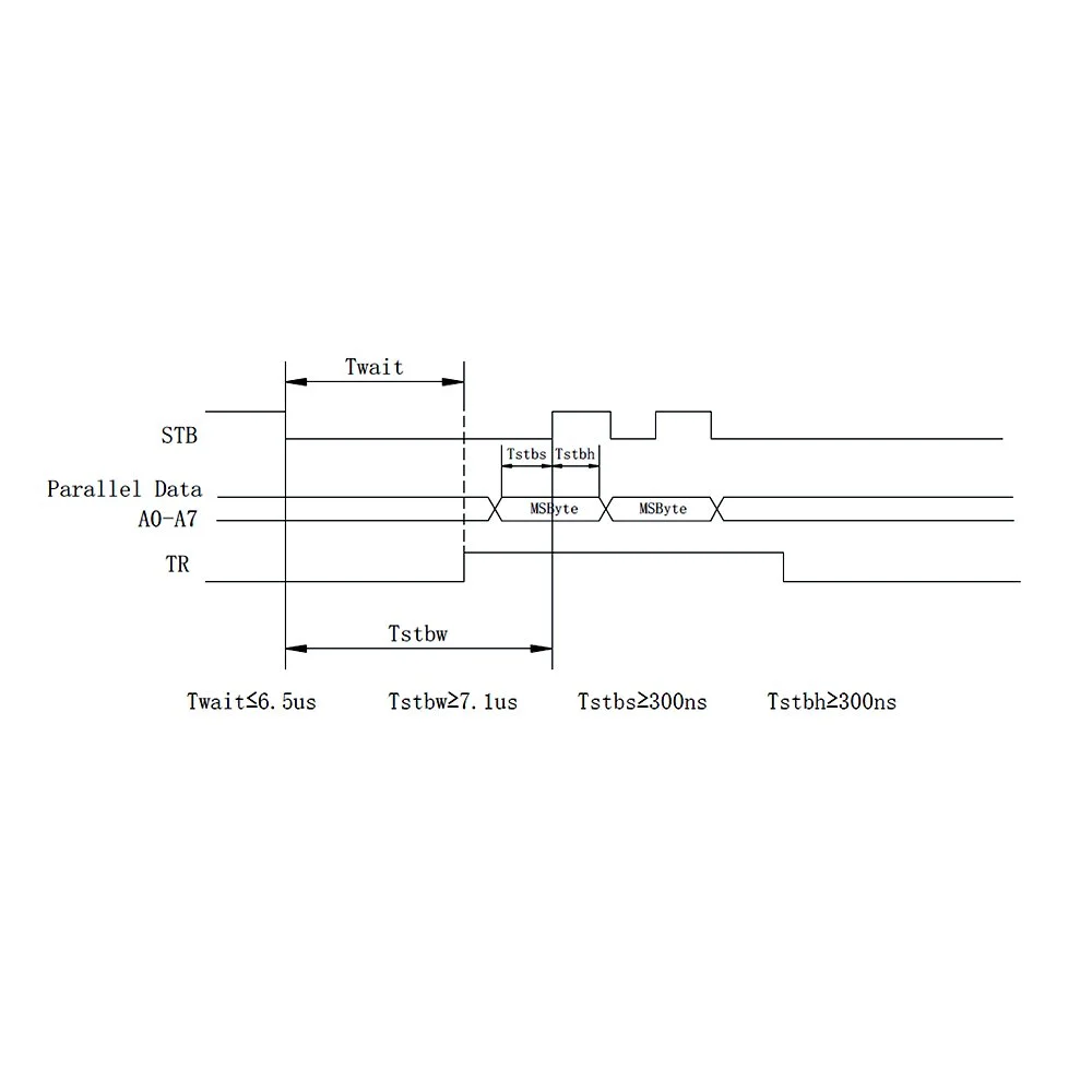 Image 4 of 9
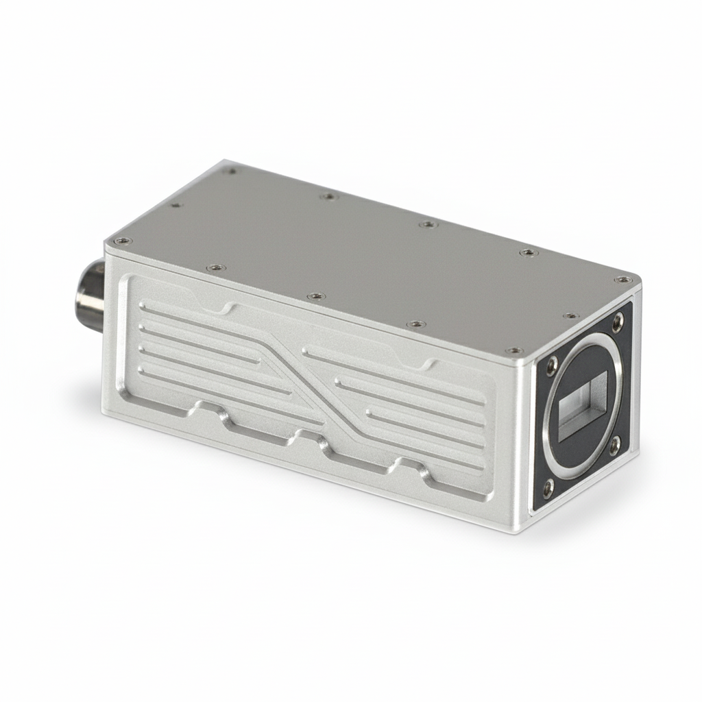
 Image 5 of 9
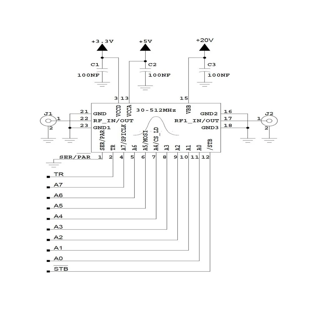 Image 6 of 9
 Image 7 of 9
 Image 8 of 9
 Image 9 of 9
Electrical Specification
| Symbol | Parameter | Min | Typical | Max | Unit |
|---|---|---|---|---|---|
| VCC | Supply Voltage | 4.75 | 5 | 5.5 | V |
| VBB | High Supply Voltage | 20 | 20 | 22 | V |
| Icc | Electric Current 1 | - | 1 | 25 | mA |
| Ibb | Electric Current 2 | - | 2 | 3 | mA |
| F | Frequency Range | 30 | - | 512 | MHz |
| I.L | Insertion Loss | - | 4 | 6 | dB |
| BW3 | 3dB Relative Bandwidth | - | 5% | 6% | MHz |
| Sel | Selectivity at F₀ ± 10% | 18 | 21 | - | dBc |
| Rf | Remote Rejection @ 2F₀ | - | 60 | - | dB |
| VSWR | Voltage Standing Wave Ratio | - | 1.5 | 2.2 | - |
| Z | Nominal Impedance | - | 50 | - | Ohm |
| BW-30dB / BW-3dB | Shape Factor | - | - | 7.5 | - |
| - | P1dB Compression Point (Output/Input) | 10 | - | - | dBm |
| t | Tuning Time | - | - | 35 | µs |
| - | Center Frequency Drift | - | - | 80 | PPM/℃ |
Handling Rating
| Symbol | Parameter | Min | Typical | Max | Unit |
|---|---|---|---|---|---|
| To | Operating Temperature | -40 | 25 | +85 | °C |
| TS | Storage Temperature | -55 | - | +105 | °C |
SPI Interface Timing
| Parameter | Description | Value | Unit |
|---|---|---|---|
| Direction | Data Transmission Direction | MSB first | - |
| FSCK | Maximum Clock Frequency | 8 | Mbps |
| MODE | SPI Mode (CPOL=0, CPHA=0) | Mode 0 | - |
| LENGTH | Data Frame Size | 16 | bits |
| IF | Interface Connection Type | 3-wire (CS, CLK, MOSI) | - |
Connecting Cable Specification
| Parameter | Description | Value | Unit |
|---|---|---|---|
| VCC | Supply Voltage | 3.3 | V |
| VBB | Supply Voltage | 22 | V |
| GND | Ground | 0 | V |
| CS | Chip Select | - | - |
| CLK | SPI Clock | - | - |
| MOSI | Master Out Slave In | - | - |
| TRIG | Output Trigger Timing | Starts after last SCLK edge | - |
Tune Command Properties
| Symbol | Band | Value | Description |
|---|---|---|---|
| fMIN | 1 | 30 MHz | Minimum tunable frequency. Absolute lowest frequency for the respective band. |
| 2 | 77.552 MHz | ||
| 3 | 216.188 MHz | ||
| fMAX | 1 | 77 MHz | Maximum tunable frequency. Frequencies beyond this result in invalid tuning. |
| 2 | 215 MHz | ||
| 3 | 512 MHz | ||
| fSTEP | 1 | 0.188 MHz | Tune step size. Minimum spacing between adjacent tune commands. |
| 2 | 0.552 MHz | ||
| 3 | 1.188 MHz | ||
| fCOM | All | - | Commanded frequency sent via SPI or parallel interface. Calculated as: (Desired Frequency − fMIN) / fSTEP, then rounded to nearest integer. Use floor for lower value or ceil for higher value selection. |
| 8.2 Tune Word Format | |||||||||||||||||
|---|---|---|---|---|---|---|---|---|---|---|---|---|---|---|---|---|---|
| (MSb) 15 |
14 | 13 | 12 | 11 | 10 | 9 | 8 | 7 | 6 | 5 | 4 | 3 | 2 | 1 | (LSb) 0 |
||
| 0 | 0 | 0 | 0 | 0 | 0 | Band Bits | Commanded Frequency | ||||||||||
| Band Bits | |||
|---|---|---|---|
| Bit 9 | Bit 8 | Selected Band | Band Range (MHz) |
| 0 | 0 | 1 | 30 – 77 |
| 0 | 1 | 2 | 77.552 – 215 |
| 1 | 0 | 3 | 216.188 – 512 |
| 1 | 1 | Unsupported, Do not Select | - |
| Frequency Calculation & Tune Command Table | ||||||||
|---|---|---|---|---|---|---|---|---|
| fDESIRED (MHz) | Req. Band | Band (Hex) | fMIN of Band (MHz) | fSTEP of Band (MHz) | fCOM Calculation (Decimal) | fCOM (Decimal) | fCOM (Hex) | Tune Command (Hex) |
| 30 | 1 | 0x00 | 30 | 0.188 | round((30 − 30) / 0.188) | 0 | 0x00 | 0x0000 |
| 53.5 | 1 | 0x00 | 30 | 0.188 | round((53.5 − 30) / 0.188) | 125 | 0x7D | 0x007D |
| 77.0 | 1 | 0x00 | 30 | 0.188 | round((77 − 30) / 0.188) | 250 | 0xFA | 0x00FA |
| 77.552 | 2 | 0x01 | 77.552 | 0.552 | round((77.552 − 77.552) / 0.552) | 0 | 0x00 | 0x0100 |
| 90.248 | 2 | 0x01 | 77.552 | 0.552 | round((90.248 − 77.552) / 0.552) | 23 | 0x17 | 0x0117 |
| 215 | 2 | 0x01 | 77.552 | 0.552 | round((215 − 77.552) / 0.552) | 249 | 0xF9 | 0x01F9 |
| 216.118 | 3 | 0x02 | 216.118 | 1.188 | round((216.118 − 216.118) / 1.188) | 0 | 0x00 | 0x0200 |
| 477.548 | 3 | 0x02 | 216.118 | 1.188 | round((477.548 − 216.118) / 1.188) | 220 | 0xDC | 0x02DC |
| Tuning Time vs Frequency & Mode | ||||
|---|---|---|---|---|
| From (MHz) | To (MHz) | Tuning Mode | Band | Tune Time (µs) @ 0 dBm |
| 30 | 77 | Parallel | 30–77 (1) | 8.3 |
| 77 | 30 | Parallel | 30–77 (1) | 9.3 |
| 77.55 | 215 | Parallel | 77.55–215 (2) | 8.3 |
| 215 | 77.55 | Parallel | 77.55–215 (2) | 9.1 |
| 216.188 | 512 | Parallel | 216.188–512 (3) | 8.3 |
| 512 | 216.188 | Parallel | 216.188–512 (3) | 9.6 |
| 30 | 215 | Parallel | BAND (1) TO BAND (2) | 8.8 |
| 215 | 30 | Parallel | BAND (2) TO BAND (1) | 10.3 |
| 30 | 512 | Parallel | BAND (1) TO BAND (3) | 8.8 |
| 512 | 30 | Parallel | BAND (3) TO BAND (1) | 9.8 |
| 215 | 512 | Parallel | BAND (2) TO BAND (3) | 5.2 |
| 512 | 215 | Parallel | BAND (3) TO BAND (2) | 5.6 |
| 30 | 77 | Serial | 30–77 (1) | 17.6 |
| 77 | 30 | Serial | 30–77 (1) | 18.6 |
| 77.55 | 215 | Serial | 77.55–215 (2) | 17.4 |
| 215 | 77.55 | Serial | 77.55–215 (2) | 19.1 |
| 216.188 | 512 | Serial | 216.188–512 (3) | 17.6 |
| 512 | 216.188 | Serial | 216.188–512 (3) | 18.3 |
| 30 | 215 | Serial | BAND (1) TO BAND (2) | 18.0 |
| 215 | 30 | Serial | BAND (2) TO BAND (1) | 19.0 |
| 30 | 512 | Serial | BAND (1) TO BAND (3) | 18.0 |
| 512 | 30 | Serial | BAND (3) TO BAND (1) | 19.0 |
| 215 | 512 | Serial | BAND (2) TO BAND (3) | 12.5 |
| 512 | 215 | Serial | BAND (3) TO BAND (2) | 14.9 |
| 14. Pin Configuration | ||
|---|---|---|
| Pin Number | Label | Description |
| 1 | SER/PAR |
Serial/Parallel Tune Command Interface Selection – Pull to VCC for SPI (serial) mode, tie to GND for parallel mode.
A power cycle is required to change modes. (Internally pulled to VCC with 10 kΩ resistor) |
| 2 | TUNE READY | Tune Ready Indicator – Normally low. Goes high when CS/STB is taken low indicating readiness for data. Returns low after data is loaded, indicating tuning is complete. |
| 3 | VCCD | Digital Interface Supply – Sets logic level (e.g., +5 V for 5 V logic, +3.3 V for 3.3 V logic). |
| 4 | A7 / SCLK |
Parallel: A7 (MSb) – Data latched on rising edge of STB. Serial: SCLK – Clock input, data latched on rising edge. (Internally pulled to VCC with 10 kΩ resistor) |
| 5 | A6 |
Parallel Data A6. (Internally pulled to VCC with 10 kΩ resistor) |
| 6 | A5 / MOSI |
Parallel: A5 data input. Serial: MOSI – Data input for tune command (16-bit). Latched on rising edge of SCLK. (Internally pulled to VCC with 10 kΩ resistor) |
| 7 | A4 / CS |
Parallel: A4 data input. Serial: CS – Active low chip select. Must be tied to STB (Pin 12) in serial mode. (Internally pulled to VCC with 10 kΩ resistor) |
| 8–11 | A3–A0 |
Parallel Data Inputs A3 (Pin 8), A2 (Pin 9), A1 (Pin 10), A0 (Pin 11). (Internally pulled to VCC with 10 kΩ resistor) |
| 12 | STB |
Serial: Wake-up control, tie to CS (Pin 7). Parallel: Controls data latching sequence. Rising edges latch MSB then LSB and trigger tuning. |
| 13 | VCC | Supply Voltage Input: 4.75 V to 5.25 V. |
| 14, 16, 18, 19, 20, 21, 23 | GND | Digital and Analog Ground. |
| 15 | VBB | High Bias Supply Voltage Input: +20 V. |
| 17, 22 | RF IN/OUT | RF Signal Input or Output. |
| Pin Name | Description |
|---|---|
| TUNE READY |
Tune Ready Indicator – The TUNE READY pin is a driven digital output. Do not connect any other push-pull output directly to this pin. The function of the TUNE READY pin is to indicate the status of the digital interface during/after tune events. The normal logic state of TUNE READY is low (de-asserted) at power-up. In this condition, the filter is ready to receive a new tune command. When a new tune command is initiated (pulling CS & STB low in serial mode or STB low in parallel mode), the TUNE READY pin transitions high (asserted) once the filter is ready to receive digital data. The external control circuit must monitor this pin or wait for the minimum control circuit setup time before loading data. After receiving a valid tune command and completing processing, TUNE READY returns to low (de-asserted). Note: In parallel mode, if TUNE READY remains high after tuning, the second rising edge of STB may have been missed. To fix this, toggle STB low for >300 ns, then high. If TUNE READY goes low, the filter can be re-tuned. |
| SER/PAR |
Serial/Parallel Command Interface Selection – This pin is sampled at power-up to determine the interface mode. Pulling SER/PAR to VCC enables SPI (serial) mode. Connecting it to GND enables parallel mode. The interface mode cannot be changed dynamically and only updates on power-up. This pin includes an internal 10 kΩ pull-up resistor to VCC. |
| CS & STB |
SPI Chip Select and Tune Strobe: Serial Mode: STB wakes the control circuitry on a low transition. For proper SPI operation, CS (pin 7) and STB (pin 12) must be tied together externally. Parallel Mode: CS is repurposed as Parallel data A4. STB wakes the control circuitry on a low transition. The next two rising edges of STB load the most significant byte (MSB) and least significant byte (LSB), respectively. |